In this Internet World, it becomes very important to shape your ideas into finished products with speed and secrecy else you will loose the opportunity to enjoy business as an advantage of being number one into the market.
Innovative Ideas gets pop-up at different levels and just due to delay in processes of shaping these ideas into products costs to company , team , an individual who owns the particular IDEA.
After taking the respective feedback through sales, marketing , voice of customer etc.. we need to shape our ideas mainly at three different levels Circuit Design, PCB Design, Prototype Testing and then Product Validation. Most of the R&D companies, Research Scholars shape the ideas into corresponding Electronic Circuit but then get trapped into vendor dependency for PCB Design & Proto PCB. This is time consuming and having a fear because a Confidential Circuit Design is been shared with an External World.
These days most of the institutions, industries where core R&D is been done are looking for a In-house Desktop Solution to Design-Simulate-Fabricate Electronic Circuits to protect an individual and organization interest to have prototype for testing and validation in minutes.This provides speed in shaping ideas into products and helps to be first in market with innovative solutions for a problem.
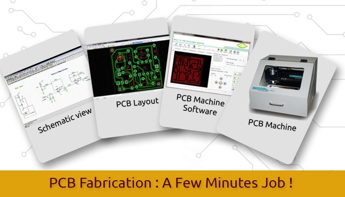
A promising solution is a combo package of Circuit & PCB Design & Simulation Software with PCB Prototyping Machine to fabricate the PCB for Prototyping Testing in few minutes. This allows to Design Circuit with built-in Component Library and then Test and do various analysis of designed circuit. We can do fault analysis by inserting faults , changing component parameters etc.. which insures the complete performance of a circuit with various possibilities of operation. The same software package allows to design PCB. The PCB Design will be exported to PCB Prototyping Machine Software on same PC and the machine removes the unwanted copper through Milling, Drills the desired holes for respective components through Drilling and cuts the PCB from the board by Routing Operation.
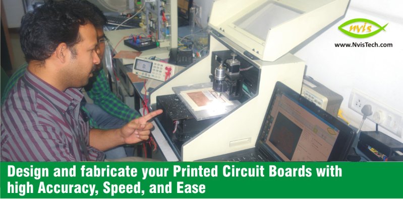
Scientech Offers Complete PCB Design Lab Model Nvis 72. The Solution has Circuit Design and Simulation Software with PCB Design Tina Design Suite. The package has more than 20,000 component library and supports all leading component manufacturers spice model Analog Devices, Fairchild, Texas an many others. It has capability of performing more than 20 different Analysis with Virtual Test & Measuring Instruments of Analog, Digital and Mixed Mode Circuits. User can insert fault and change the component parameter to see the effect on circuit performance. Built-in PCB Design is a value added feature to design the well tested circuit and see 3D View from Component & Solder Side to insure proper component and track placement. PCB Machine takes the design details as an input and fabricates the PCB in minutes without using any Chemicals. It removes Unwanted Copper, Does proper Drilling for Components, and Cut the Fabricated PCB in few minutes.
You may like to down load technical details of such promising solution from the following link
http://www.nvistech.com/technical-training/pcb-lab/pcb-prototype-machine